
key steps in PCB fabrication and assembly
The process of PCB fabrication and assembly is intricate and involves multiple steps to ensure the final product is functional, reliable, and meets specific design requirements. These steps transform a basic idea or schematic into a fully operational printed circuit board (PCB) ready for integration into electronic devices. The key steps in PCB fabrication and assembly are critical to ensuring the quality and performance of the finished product.
The first step in pcb fabrication and assembly is the design phase, where the circuit layout is created using specialized PCB design software. This design specifies the arrangement of electrical components, the connections between them, and the overall structure of the PCB. The design is then reviewed and tested virtually to identify potential issues before the actual fabrication process begins. Once the design is approved, it is converted into a format that can be used by the fabrication machinery, such as Gerber files, which contain detailed instructions for each layer of the PCB.
In the fabrication stage, the next step is preparing the copper-clad laminate, which serves as the base material for the PCB. This laminate is typically made of a combination of fiberglass and resin and is covered with a thin layer of copper on both sides. The copper layer will form the electrical traces and pads that connect the components. The copper laminate is then cleaned and prepared for the next stage of the process.
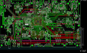
What are the key steps in PCB fabrication and assembly?
The design pattern is transferred onto the copper laminate through a photolithographic process. In this step, a photosensitive film is applied to the copper surface, and ultraviolet (UV) light is used to expose the film through a photomask that mirrors the PCB design. The areas exposed to UV light harden, while the unexposed areas remain soft. These soft areas are then washed away, leaving behind the desired copper pattern. This process is critical to achieving precise electrical connections between components, ensuring the functionality of the PCB.
Next, the PCB undergoes an etching process. This involves using a chemical solution to remove the unwanted copper from the board, leaving only the copper traces that make up the electrical paths. After etching, the board is thoroughly cleaned to remove any residual chemicals. At this point, if the design calls for a multi-layer PCB, additional layers of copper and insulating material are added, and the process is repeated to create the necessary layers of circuitry.
Following etching, a protective solder mask is applied to the PCB. The solder mask acts as a barrier to prevent the solder from bridging between copper traces during the assembly process. This protective layer also ensures that the board remains clean and free from contaminants, which could affect the performance of the PCB. After the solder mask is applied, the PCB is printed with a silkscreen layer, which includes important markings such as component labels and test points.
Once the fabrication process is complete, the PCB moves to the assembly phase. This step involves placing and soldering the electronic components onto the board. Components such as resistors, capacitors, microchips, and connectors are placed on the PCB using either manual or automated methods. Automated pick-and-place machines are commonly used for high-volume production to accurately position components in their designated locations. After the components are placed, the PCB undergoes a soldering process, where heat is applied to melt solder and form electrical connections between the components and the copper traces. This can be done through wave soldering, reflow soldering, or other methods, depending on the components and the complexity of the design.
Finally, the assembled PCB undergoes a thorough inspection and testing phase. Visual inspections, automated optical inspection (AOI), and electrical tests are performed to ensure that the PCB functions as intended. Any defects such as soldering issues, missing components, or incorrect placements are identified and corrected before the PCB is considered ready for shipment.
