
design considerations for pcb board
PCBs are used in electronic devices to connect and integrate circuit components. These boards have several design considerations that influence their performance and reliability. These include routing, thermal management, and electromagnetic interference (EMI). PCBs are usually rectangular but can be made in other shapes depending on the application. The materials and components used in a PCB can also impact its design.
The routing of traces is a crucial aspect of pcb board layout. These tracks, typically made of copper, provide the path for electrical current to flow between components. Choosing the right routing strategy is essential to ensuring the integrity of high-speed signals.
A PCB’s material, rigidity, and thickness all play a role in its routing strategy. For example, a thinner board can be less likely to be bent than a thicker one. In addition, thin boards can be designed to have a greater number of layers, which may increase its performance.
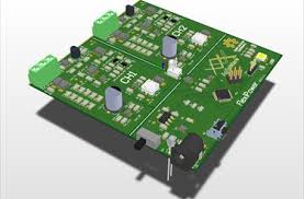
What are the design considerations for pcb board
Keeping track of the amount of heat a board generates is also important. Excessive temperatures can lead to component failures and shorten a board’s lifespan. To prevent this, a designer must consider the thermal management of the board, including incorporating thermal vias and using appropriate heat sinks.
In addition to power and ground planes, a PCB should have signal planes. These planes return the signals routed on traces and can degrade the performance of a circuit if they aren’t properly designed. To prevent this, designers should ensure that the signal planes are symmetrical and have enough space to meet the requirements of the circuit’s components.
Another critical aspect of the routing process is maintaining a proper clearance between conductive elements. This is necessary to protect against arcing or short circuits and can be determined by measuring the distance between two conductive surfaces along the length of an insulating layer. The required clearance depends on the voltage level, insulating material, and environmental conditions.
Finally, a PCB should be properly tested. This includes checking for voids, solder joints, and thermal stress. It’s also a good idea to test the sensitivity of high-speed signals and verify that components can be placed close together without causing problems.
A final important consideration is making sure that the PCB design complies with the manufacturer’s guidelines. These rules may include a minimum trace width and spacing, maximum clearance between tracks, and tolerances for drill holes and copper thickness. Taking these considerations into account can help ensure that the board can be produced reliably and efficiently.
The first step in a successful PCB design is the pre-layout process, which refers to the arrangement of layers that make up the board. The stack-up is the arrangement of the different layers that comprise the PCB, which includes overlays, solder masking, and dielectric layers. During the pre-layout stage, designers should choose the optimal materials and components for the project and ensure that these items are available. This can be difficult because some components and materials are hard to find and expensive, so it is important to do your research before committing to anything.
