
Limitations of PCB
A rigid flex PCB is a versatile design option that saves space and reduces weight in electronic devices. These circuit boards can also withstand harsh environmental conditions and are used in many technological applications. However, a rigid flex PCB is not without its limitations. Understanding these limitations can help designers and fabricators create more reliable rigid flex circuit boards.
One limitation of pcb flex rigid is that it requires higher costs to produce due to the complex manufacturing processes involved. This type of circuit board is also more difficult to test and inspect. Therefore, it is important for designers to work with a reputable manufacturer and follow good design practices.
The first step to designing a robust pcb flex rigids is to establish an optimal layer stack. This includes ensuring that there is symmetry and balance in the copper distribution and dielectric materials. It is also essential to pair signal layers with reference planes to minimize signal coupling and control impedance in flex areas. In addition, it is vital to include dummy layers in the flex area to ensure that there are no discontinuities or voids in the flex portion of the circuit board.
Limitations of PCB Flex Rigid
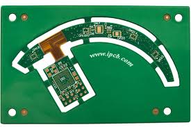
Another limitation of pcb flex rigid that should be considered is the transition zone between the flexible and rigid sections of the circuit board. This section is prone to a number of defects, including adhesive squeeze-out, protrusion of dielectric materials, and haloing. This can damage the conductor paths in the flexible portion of the circuit. It is important for designers to extend the flex coverlay into the rigid section to avoid these issues. Additionally, they should ask their CM to apply flexible epoxy strain relief and a bead of epoxy material at the transition zone to increase bend reliability.
Other limitations of pcb flex rigid include the need to ensure that the flex and rigid sections can withstand repeated bending and flexing without mechanical failure. This can be achieved by using the proper thickness of stiffeners and routing signals in a straight, perpendicular line near the bend point. In addition, it is important to route traces in a manner that minimizes sharp corners.
A rigid flex circuit board should also include sufficient thermal dissipation to protect the electrical components from overheating. This can be accomplished by using heat sinks and thermal vias, as well as by routing traces away from power-generating components and conducting them through the flex area to prevent overheating.
A rigid flex circuit board can also be damaged by a sudden alteration in trace width near pads and vias. This can occur when a designer fails to follow proper bending guidelines or neglects to consider the possibility of stacked traces in the flex and bendable sections of the circuit board. To overcome these challenges, it is important to use the correct tolerances in the flex and bendable sections of your design, as well as to avoid placing stiffeners too close to pins or vias.
