
How Does Flex PCB Fabrication Support High-Density Connections?
In the realm of modern electronics, high-density connections are essential for meeting the increasing demand for miniaturization and performance. As devices become more powerful and compact, the ability to fit more components into smaller spaces has become critical. Flex PCB fabrication plays a pivotal role in supporting high-density connections, allowing manufacturers to design flexible printed circuit boards (PCBs) that not only fit into tight spaces but also ensure reliable electrical performance. This capability is particularly important in industries such as consumer electronics, automotive, medical devices, and telecommunications, where miniaturized components are integral to the device’s functionality.
The Importance of High-Density Connections
High-density connections refer to the ability to place a large number of circuit traces, components, and interconnections within a limited area. This is particularly challenging when designing for small, portable, or space-constrained devices. Traditional rigid PCBs often face limitations in routing and space optimization, which is where flex PCB fabrication comes into play. Flex PCBs can be bent, twisted, and folded into various shapes, enabling designers to achieve higher circuit densities without compromising the integrity of the connections or the performance of the device.
How Flex PCBs Enable High-Density Connections
Flexible Design for Compact Layouts
One of the main advantages of flex pcb fabrication in supporting high-density connections is its inherent flexibility. Unlike rigid PCBs, flex PCBs can be folded or rolled into compact shapes that take up less space. This allows for more efficient use of the available area, enabling designers to arrange components and circuit traces more densely. As a result, high-density connections can be achieved without sacrificing the mechanical integrity of the device. This flexibility also makes it easier to design complex, multi-dimensional interconnections that would be impossible with a rigid PCB.
Layer Stacking for Increased Density
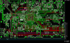
Flex PCBs can incorporate multiple layers to accommodate more circuit traces and components within a small footprint. Through flex PCB fabrication, it’s possible to create multi-layer flex PCBs, where the different layers are stacked together to provide more routing space. This allows for higher-density connections between components, as each layer can be dedicated to specific functions or signals. By using this multi-layer approach, manufacturers can achieve the high-density interconnections necessary for complex devices like smartphones, wearables, and other compact electronics.
Smaller Trace Sizes
Another key feature of flex PCB fabrication is the ability to create narrower traces and smaller vias than those possible with traditional rigid PCBs. The advanced techniques used in flex PCB manufacturing allow for fine-pitch connections and more tightly packed circuits. This is crucial for achieving high-density designs, as smaller traces and vias allow more components to be placed on the same board without interfering with one another. These miniaturized connections make it possible to achieve higher performance while keeping the device compact.
Improved Signal Integrity
Maintaining signal integrity is critical when dealing with high-density connections, as signal degradation can occur when circuits are densely packed together. Flex PCB fabrication offers significant advantages in this regard. The flexible nature of the board helps reduce the length of the signal paths and minimizes the number of connections required. Additionally, the ability to create tightly controlled impedance and shield sensitive signals from external interference ensures that signal integrity is maintained even in high-density designs. This is especially important in high-speed applications like telecommunications and high-performance computing, where signal quality is paramount.
Advanced Component Placement and Routing
Flex PCB fabrication also allows for more efficient component placement and routing compared to rigid PCBs. By leveraging the flexibility of the material, designers can place components on both sides of the board, as well as integrate components along the flexible substrate itself. This frees up valuable space for additional components or high-density traces, further enhancing the overall design. The compactness and flexibility of flex PCBs enable tighter routing of high-density connections, ensuring that all components are properly connected and functioning.
Conclusion
In conclusion, flex PCB fabrication is a crucial enabler of high-density connections in modern electronics. The ability to create flexible, multi-layered, and high-performance circuits in compact form factors allows for innovative designs in a variety of industries. By supporting smaller trace sizes, more efficient routing, and better signal integrity, flex PCBs provide an ideal solution for devices that require high-density interconnections without compromising on performance. As electronics continue to evolve towards smaller and more complex designs, the role of flex PCB fabrication in supporting high-density connections will only continue to grow.
