
RF PCBs handle high-power signals
Radio Frequency (RF) PCBs are designed to manage signals at various frequencies and power levels, ranging from low-power signals in mobile devices to high-power signals used in radar, satellite communication, and broadcasting systems. High-power RF signals present particular challenges for PCB design due to their tendency to cause excessive heat, signal distortion, and electromagnetic interference (EMI) if not handled correctly. Therefore, managing high-power signals in RF PCBs requires careful design considerations, including power handling capacity, thermal management, impedance matching, and the use of appropriate materials to ensure signal integrity and prevent system failure.
One of the primary concerns when handling high-power RF signals is thermal management. High-power RF signals generate significant heat as they travel through the circuit, and this heat must be dissipated to prevent the PCB and its components from overheating. Overheating can lead to signal loss, degradation, and even component failure. To address this, rf pcb designed for high-power applications often incorporate heat sinks, thermal vias, and large ground planes to effectively spread and dissipate heat. Thermal vias, for example, are small holes in the PCB that connect the top and bottom layers of the board, allowing heat to be transferred from hot components to a heat sink or the lower layers of the PCB. By incorporating these design features, engineers can ensure that high-power signals are managed without causing damage to the PCB or degrading performance.
Another crucial aspect of handling high-power RF signals is impedance matching. RF circuits require precise impedance matching between components, transmission lines, and the PCB itself to ensure that signals are transmitted efficiently without reflection or loss. Mismatched impedance can result in signal reflections, which not only reduce signal strength but also increase the likelihood of signal distortion and interference. To manage high-power signals, RF PCB designs often include carefully designed microstrip lines or stripline transmission lines that maintain consistent impedance throughout the signal path. In some cases, impedance-matching networks, including capacitors and inductors, are integrated into the PCB design to ensure proper signal transmission and minimize the risk of signal loss or distortion.
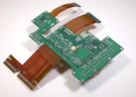
How do RF PCBs handle high-power signals?
Material selection is another critical consideration in handling high-power RF signals. The choice of PCB material affects the board’s ability to handle power, maintain signal integrity, and dissipate heat effectively. For high-power applications, engineers typically select low-loss dielectric materials with stable thermal properties and low resistance to ensure minimal signal attenuation and heat buildup. Materials like Teflon (PTFE), RO4000 series, or ceramic-filled composites are commonly used in high-power RF PCBs because of their excellent thermal conductivity, low loss factors, and high dielectric strength, making them suitable for handling high-frequency, high-power signals. These materials not only reduce signal loss but also help maintain signal clarity while providing the necessary power handling capacity.
In addition to material selection, component choice is essential when designing RF PCBs for high-power signals. Power amplifiers, for example, need to be selected carefully to ensure they can handle the high-power levels required by the system. These components must be designed with heat dissipation features and optimized for high-efficiency performance to prevent overheating. Additionally, low-profile components such as capacitors, resistors, and inductors must be chosen to withstand the high voltages and currents associated with high-power RF signals without degrading over time.
Shielding also plays an important role in managing high-power RF signals. High-power RF circuits can generate significant amounts of electromagnetic interference (EMI), which can affect nearby components and systems. To reduce EMI, shielding techniques are often used to encapsulate sensitive components or high-power signal paths in metallic enclosures or conductive coatings. This prevents unwanted signals from radiating out of the PCB and interfering with adjacent components, while also protecting the PCB from external sources of interference. Shielding helps maintain signal integrity by preventing distortion and ensuring that the signal transmitted through the PCB remains clear and undistorted.
Finally, high-power RF PCBs often incorporate power management techniques to ensure stable operation and prevent damage to sensitive components. These include the use of current-limiting devices such as resistors or fuses to prevent excessive current flow and voltage regulators to maintain a stable voltage supply. By managing the power input and distribution across the PCB, engineers can ensure that the system operates within its design parameters, preventing power surges or fluctuations that could damage the board or lead to performance degradation.
In conclusion, RF PCBs designed to handle high-power signals rely on a combination of advanced design strategies, material selection, and thermal management techniques to ensure the integrity and reliability of the system. By addressing challenges related to heat dissipation, impedance matching, signal integrity, and power management, engineers can create robust RF PCBs that effectively handle high-power signals while maintaining optimal performance and minimizing the risk of damage or distortion.
