
Flex PCB Assembly Tips
Flex PCBs are rapidly gaining in popularity as a highly versatile component for modern electronic devices. Their ability to bend, twist, and compress while maintaining electrical specifications and functionality streamlines production processes, minimizes pcb manufacturing costs, and offers a high-performance solution for a wide range of applications. However, integrating a flexible circuit requires careful consideration of the layer configurations and stack-ups used in the design. Collaborating with a knowledgeable fabricator and following industry guidelines can greatly simplify this process, ensuring the optimal outcome for your project.
The etching and bonding methods involved in a flex circuit are significantly different from those of a rigid board, making it essential to follow a rigorous design-for-manufacture process to ensure your final product meets all electrical requirements. This is especially true for multi-layer flex boards, which can be difficult to assemble without proper preparation. To maximize your flex circuit’s efficiency and reliability, consider the following tips:
When it comes to the stack-up of a flex PCB, consistency is key. The layer arrangement must be consistent throughout the board to prevent crosstalk and ensure that the copper is evenly distributed. In addition, it is recommended that the traces be routed perpendicular to the bend area to eliminate stress concentration points that can cause copper fatigue over time.
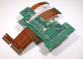
Flex PCB Assembly Tips for Multi-Layer Designs
Another important factor to consider when constructing a flex circuit is the amount of clearance between holes and the surrounding copper. A large hole-to-copper clearance can cause the copper to detach from the plate during bending. To avoid this issue, ensure that the drill-to-copper distance is at least 8 mil. It is also advised to include annular rings around the holes to improve mechanical strength.
Lastly, when routing your traces near the bend area, it is crucial to keep the areas clear of discontinuities such as vias, cutouts, and slits. These can create stress points that result in cracking and tearing during flexing. Instead, incorporating circular sections (relief holes) into these areas can reduce the stress that is applied to the traces.
Adhesive materials: Acrylic adhesives, epoxy adhesives, and pressure-sensitive adhesives (PSA) are the most common types of adhesives that can be used in a flex pcb production. These adhesives are flex-compatible and provide excellent adhesion to a variety of substrates. Additionally, they offer a solderable surface and inhibit copper oxidation.
Stiffener material: Localized rigid material known as stiffeners can be added to single-sided, double-sided, and multi-layer flex circuits to increase their strength, thickness, and rigidity in specific areas of the board. Stiffeners are typically made of materials like FR4, Kapton, or aluminum and can be attached using pressure-sensitive or acrylic thermally cured adhesives. They can be used for a variety of purposes including strain relief, weight balance, heat dissipation, and preventing connections from cracking.
