
Using Pcb Design and Assembly Technology
Printed circuit boards (PCBs) are the heart of electronic devices. Their purpose is to translate a schematic into a functional device. It is important for manufacturers to choose the right PCB design and assembly service to meet their project needs. It’s also vital to maintain open communication and a positive relationship with the chosen company to ensure success. This article will explore the advantages of using Pcb design & assembly technology and how to find the best partner for your business.
Essentially, a PCB assembly involves inserting components into plated holes on a circuit board. These components are then soldered together with a specialized soldering process. Depending on the type of components, there are different methods used to do this. Some methods are more efficient than others, but all require a skilled operator. Some of the more common techniques include wave soldering and selective soldering.
In order to assemble PCBs, it is first necessary to create the component footprints. These must be created accurately based on the land patterns specified in each integrated component’s datasheet. Otherwise, there could be problems with the circuit board’s functionality and/or manufacturability. For instance, incorrect footprints may cause uneven heating of the component. This can result in shorts and other malfunctions.
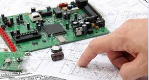
Advantages of Using Pcb Design and Assembly Technology
Another key factor in the pcb design & assembly process is the placement of vias. These are pathways between layers that improve signal performance and make it easier for the assembler to test and debug the circuit board. This step also reduces the number of connections and components, which decreases the overall cost of the circuit board.
Assemblers must also ensure that the polarity of all components is marked properly. This can help eliminate mishaps during the reflow or wave soldering processes. They must also verify that the traces are properly spaced to prevent crosstalk between traces. Finally, the assembler must make sure that all of the appropriate tools and equipment are available. This is particularly important for large batches of PCBs.
Once the assembler has verified that all of the components are in place, they can then perform final testing to confirm that the circuit board functions correctly. This can be done with an AOI machine, which uses cameras to inspect the assembled circuit board at various angles. This allows the assembler to identify low-quality solder and other defects that can cause issues later in the production process. Once all of these steps have been completed, the circuit boards are then cleaned and packaged for shipping.
This step helps to remove flux residues, stains, oil and fingerprints from the boards before they are shipped out for customer use. This ensures that the assembler’s customers receive high-quality products. In addition, it can protect the assembler from liability claims for product failures caused by improper assembly or installation. This will ultimately lead to better customer satisfaction and increased revenue for the assembler.
